Nitrogen-Vacancy Centers: Engineering Optically Addressable Solid-State Spin Qubits in Diamond Lattices
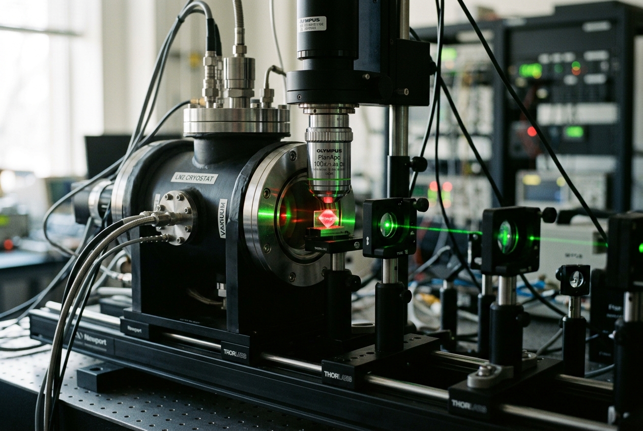
The global race to construct a functional quantum computer is widely portrayed as a battle waged at the extremes of absolute zero. In laboratory basements from Zurich to Santa Barbara, colossal stainless-steel cryostats—known colloquially as dilution refrigerators—pump liquefied helium isotopes around the clock. Their purpose is to chill fragile superconducting electrical circuits down to fractions of a degree above absolute zero, colder than the deep vacuum of interstellar space. The moment ambient thermal energy infiltrates these systems, their delicate quantum states dissolve into meaningless classical noise.
Yet, embedded inside common industrial gemstones lies a radical alternative that operates not in cryogenic isolation, but on a laboratory benchtop at room temperature.
Within the rigid, crystalline lattice of diamond, single atomic defects known as nitrogen-vacancy (NV) centers can trap individual electrons and isolate their quantum properties at ambient temperatures and pressures. These atom-scale imperfections can be initialized, manipulated, and read out using standard green laser pointers and everyday microwave electronics.
The implications of this physical reality are profound. If quantum information processing can thrive within a solid gemstone without the logistical encumbrance of cryogenic refrigeration, the barriers preventing quantum technology from entering hospitals, field geology, telecommunications networks, and everyday computing shrink dramatically. From non-invasive magnetic imaging of single living cancer cells to building unhackable continental communication networks, the nitrogen-vacancy center represents one of the most versatile solid-state platforms in modern physics.
+--------------------------------------------------------------------------------------------------+
|                                     THE ATOMISTIC LANDSCAPE                                      |
|                                                                                                  |
|         Diamond Carbon Lattice                      The Nitrogen-Vacancy (NV) Defect             |
|                                                                                                  |
|            (C) --- (C) --- (C)                            (C) --- (C) --- (C)                    |
|             |       |       |                              |       |       |                     |
|            (C) --- (C) --- (C)                            (C) --- (N) --- (C)  <- Nitrogen Atom  |
|             |       |       |                              |       |                             |
|            (C) --- (C) --- (C)                            (C) --- [V] --- (C)  <- Vacancy (Void) |
|             |       |       |                              |       |       |                     |
|            (C) --- (C) --- (C)                            (C) --- (C) --- (C)                    |
|                                                                                                  |
|   Pure Diamond: Transparent insulator.           Defect Center: Traps 2 electrons; acts as a     |
|   Rigid, spin-free carbon-12 matrix.             controllable "artificial atom" in solid state.  |
+--------------------------------------------------------------------------------------------------+
2. The Idea in Plain English
To understand why a defect in diamond functions as a quantum computer, consider the architecture of a perfect diamond crystal. Diamond is composed of carbon atoms arranged in an exceptionally rigid, repeating three-dimensional tetrahedral lattice. In its purest form, diamond is an electrical insulator: transparent, chemically inert, and silent.
Now, imagine plucking out two adjacent carbon atoms from this perfect lattice. In place of the first carbon atom, we substitute a single nitrogen atom (which has five valence electrons rather than carbon's four). In place of the second carbon atom, we leave an empty structural void—a vacancy.
This combined pairing—a substitutional nitrogen atom situated directly adjacent to a lattice vacancy—is called a nitrogen-vacancy center.
In its most technologically useful configuration, this defect captures an extra electron from the surrounding crystal lattice, creating the negatively charged state denoted as $\text{NV}^-$. This vacancy acts like an atomic cage, trapping a pair of unpaired electrons within the crystal gap. Because diamond’s carbon framework is so chemically stiff and magnetically quiet, the trapped electrons behave as though they were suspended in an ultra-high vacuum chamber, insulated from the chaotic thermal vibrations of the outside world.
       [ Classical Bit ]                         [ Quantum Bit (Qubit) ]

         +-----------+                             |0> (Spin Up)
         |   0 / 1   |                                  ^
         +-----------+                                  |    . - ~ - .
                                                        |  /     |     \
     Definite State Only:                               | /      |      \
     A coin resting flat on                             +--------+------->  |1> (Spin Down)
     a table (Heads or Tails).                           \       |      /
                                                          \      |     /
                                                            ` - ~ - '
                                                    Continuous Superposition:
                                                    A coin spinning in mid-air.
In classical computation, a bit is a physical switch that exists in one of two deterministic states: 0 or 1. A quantum bit, or qubit, exploits the quantum mechanical property known as spin—an intrinsic form of angular momentum carried by fundamental particles.
You can visualize an electron's spin as a microscopic magnetic compass needle. In the classical world, the needle points either north (representing 0) or south (representing 1). In the quantum realm, however, the compass needle can point north, south, or exist in a superposition where it points in both directions simultaneously, like a coin spinning continuously on a table until it is observed.
By addressing this single atomic defect with targeted pulses of green laser light and microwave radiation, physicists can steer this microscopic compass needle with exquisite mathematical precision, writing, processing, and retrieving quantum information stored directly inside the gemstone.
3. How It Actually Works — The Mechanics
To comprehend the operation of the NV center, we must examine its atomistic symmetry, its electronic state manifold, and the optical pathways that enable state initialization and readout.
                                  ELECTRONIC ENERGY LEVEL DIAGRAM

             Triplet Excited State (3E)
             +------------------------------------------------------+
             |  m_s = 0                        m_s = +1, -1         |
             +------------------------------------------------------+
                     ^     |                       |           |
      532 nm Pump    |     | 637-800 nm            |           | Fast Non-Radiative
      (Off-Resonant) |     | Radiative             |           | Intersystem Crossing
                     |     | Fluorescence          |           v
                     |     v                       |    +---------------+
                     |   (BRIGHT)                  |    | Singlet (1A1) |
                     |                             |    +---------------+
                     |                             |            |
                     |                             |            | ~300 ns Metastable
                     |                             |            v
                     |                             |    +---------------+
                     |                             |    |  Singlet (1E) |
                     |                             |    +---------------+
                     |                             |            |
                     |                             |            | Preferential Decay
                     |                             v            v
             +------------------------------------------------------+
             |  m_s = 0                        m_s = +1, -1         |
             +------------------------------------------------------+
                     | <------- D = 2.87 GHz -------> |
                     |         (Zero-Field)           |
                     |                                |
                     +--- [Microwave Control Pulse] --+

             Triplet Ground State (3A2)
Atomistic Structure and $C_{3v}$ Symmetry
The negatively charged NV center consists of the substitutional nitrogen atom, the neighboring vacancy, and six localized electrons (three supplied by the dangling carbon bonds surrounding the vacancy, two from the nitrogen atom, and one captured from the diamond lattice donor pool). The symmetry of this geometric arrangement belongs to the trigonal pyramidal point group, designated in crystallographic notation as $C_{3v}$ according to standard group theory in physics.
The symmetry axis of the defect lies along the crystallographic $\langle 111 \rangle$ direction of the diamond lattice, forming an intrinsic quantization axis for electron spin.
The Electronic Manifold and Spin Ground State
The electronic ground state is an orbital singlet with spin triplet character, denoted as $^{3}A_2$ ($S = 1$). Because of spin-spin dipole interactions between the two unpaired electrons, the ground state experiences an intrinsic energy splitting even in the total absence of an external magnetic field. This is known as zero-field splitting ($D$).
The ground state Hamiltonian describing this interaction is formulated as:
$$H_{\text{ground}} = D S_z^2 + g_e \mu_B \mathbf{B} \cdot \mathbf{S} + \mathbf{S} \cdot \mathbf{A} \cdot \mathbf{I}$$
Where: * $D \approx 2.87\text{ GHz}$ represents the axial zero-field splitting parameter at room temperature ($300\text{ K}$). * $S_z$ is the electron spin-1 operator projected along the defect axis. * $g_e \approx 2.0028$ is the Landé g-factor of the electron, and $\mu_B$ is the Bohr magneton. * $\mathbf{B}$ is the external static magnetic field vector, lifting the degeneracy of the $m_s = \pm 1$ states via the Zeeman effect. * $\mathbf{A}$ is the hyperfine tensor describing coupling to local nuclear spins $\mathbf{I}$ (such as the central $^{14}\text{N}$ or $^{15}\text{N}$ nucleus).
In simple terms: even when no external magnetic fields are applied, the state where the electron spin projection is zero ($m_s = 0$) sits at a lower energy than the states where the spin projection is aligned or anti-aligned ($m_s = +1$ and $m_s = -1$). The energy difference between them corresponds precisely to a microwave frequency of $2.87\text{ gigahertz}$.
Optical Spin Initialization via Intersystem Crossing
The ability to initialize a quantum state into a known pure state is an absolute prerequisite for quantum computing, as formalized in the DiVincenzo criteria. The NV center accomplishes this optically through an elegant quantum shortcut called intersystem crossing (ISC).
- Optical Excitation: When the defect is illuminated with off-resonant green laser light (wavelength $\lambda = 532\text{ nm}$), electrons in the $^{3}A_2$ ground state absorb photons and transition into the excited orbital triplet state, designated as $^{3}E$. This optical transition is spin-conserving ($\Delta m_s = 0$).
- Radiative Decay: From $^{3}E$, the electron can drop directly back to $^{3}A_2$ by emitting a red photon (in a spectral band spanning from the zero-phonon line at $637\text{ nm}$ out to $800\text{ nm}$ due to lattice phonon sidebands).
- The Non-Radiative Bypass: Crucially, an alternative non-radiative relaxation pathway exists. Electrons excited into the $m_s = \pm 1$ sublevels of the $^{3}E$ state experience strong spin-orbit coupling, which diverts them into a pair of intermediate singlet states ($^{1}A_1$ and $^{1}E$).
- Preferential Decay: Once trapped in the singlet manifold (which has a relatively long metastable lifetime of $\sim 300\text{ ns}$), the electrons do not emit red luminescence. Instead, they decay predominantly into the $m_s = 0$ ground state.
Because electrons starting in $m_s = \pm 1$ are systematically filtered through this dark singlet pathway and dumped into $m_s = 0$, continuous green illumination for just a few hundred nanoseconds forces the electron spin population into the pure $m_s = 0$ state with an efficiency exceeding $90\%$.
Optically Detected Magnetic Resonance (ODMR) Readout
This asymmetric decay pathway also yields a straightforward mechanism for state readout. When the NV center resides in the $m_s = 0$ state, it cycles continuously through the bright radiative transition, emitting a high flux of red photons. When it resides in $m_s = \pm 1$, it is frequently diverted into the dark singlet state, causing a marked reduction ($\sim 30\%$) in emitted fluorescence.
By measuring the rate of detected red photons under laser illumination, an experimentalist can immediately determine the quantum state of the single electron spin. When a resonant microwave field ($2.87\text{ GHz}$) drives transitions between $m_s = 0$ and $m_s = \pm 1$, the observed red fluorescence visibly dips—a technique pioneered in scientific literature known as Optically Detected Magnetic Resonance (ODMR), thoroughly documented in research published across Nature and peer-reviewed journals.
       FLUORESCENCE INTENSITY PROFILE UNDER APPLIED MICROWAVE FREQUENCY

       Photons Detected
            ^
            |
       Max -+-------+                                     +-------
            |        \                                   /
            |         \                                 /
            |          \                               /
            |           \                             /
       Min -+            \                           /
            |             +                         +
            |             |                         |
            |             v                         v
            +-------------+-------------------------+-------------> Microwave
                       2.85 GHz                  2.89 GHz          Frequency
                      (m_s = -1)                (m_s = +1)

            Dip occurs when microwave frequency matches transition energy,
            transferring electrons into darker m_s = +/- 1 states.
Coherent Microwave Manipulation and Dynamical Decoupling
Once initialized into the $m_s = 0$ ground state, resonant microwave magnetic fields ($B_1 \cos(\omega t)$) are applied via micro-fabricated coplanar waveguides to coherently steer the electron spin vector around the Bloch sphere. By applying a calibrated microwave pulse of duration $\tau$, physicists induce Rabi oscillations, creating deterministic superpositions such as:
$$|\psi\rangle = \frac{1}{\sqrt{2}} \left(|m_s = 0\rangle + |m_s = -1\rangle\right)$$
However, a raw quantum superposition suffers from dephasing caused by magnetic field fluctuations from surrounding isotopic impurities in the diamond (primarily carbon-13 nuclei, which possess an uncontrollable nuclear magnetic spin of $I = 1/2$). The bare inhomogeneous dephasing time, denoted $T_2^*$, is typically limited to a few microseconds in natural diamond.
To protect the quantum bit from environmental noise, physicists apply dynamical decoupling pulse sequences, such as the Carr-Purcell-Meiboom-Gill (CPMG) or XY8 protocols.
                               CPMG PULSE SEQUENCE TIMING

Microwave:   (pi/2)x         (pi)y         (pi)y         (pi)y         (pi/2)x
Pulses          |              |             |             |              |
                |<--- tau ---->|<-- 2*tau -->|<-- 2*tau -->|<--- tau ---->|

Spin Phase:     [Superposition]  [Inversion]   [Inversion]   [Inversion]  [Projection]
Accumulation:   + delta phi      - delta phi   + delta phi   - delta phi  = Zero Net Noise
A dynamical decoupling sequence functions like an ultra-fast noise-canceling headphone for quantum spins: 1. An initial $(\pi/2)$ pulse tips the spin into the equatorial plane of the Bloch sphere. 2. The spin precesses freely for a duration $\tau$, accumulating unwanted phase noise from background magnetic fluctuations ($+\delta\phi$). 3. A sequence of calibrated $(\pi)$ inversion pulses periodically flips the spin by $180^\circ$ at intervals of $2\tau$. 4. During the second half of the cycle, the environmental noise accumulates with an inverted sign ($-\delta\phi$), canceling out the net random phase drift.
By applying these multi-pulse control sequences, the phase coherence time $T_2$ of the electron spin can be extended from microseconds to over one second at room temperature, and several minutes at cryogenic temperatures.
Multi-Qubit Nuclear Spin Registers
While the electron spin provides an agile interface for optical initialization and microwave gating, its strong magnetic dipole moment makes it susceptible to ambient disturbances. To build multi-qubit registers, physicists exploit the NV center’s electron spin as a central processor to manipulate surrounding nuclear spins ($^{14}\text{N}$, $^{15}\text{N}$, and proximate $^{13}\text{C}$ atoms).
Because atomic nuclei are shielded behind dense electron clouds, their magnetic dipole moments are roughly three orders of magnitude smaller than that of an electron. Consequently, nuclear spins interact very weakly with the environment, acting as pristine, ultra-long-lived quantum memory banks capable of preserving quantum coherence for hours.
Using the hyperfine interaction ($\mathbf{S} \cdot \mathbf{A} \cdot \mathbf{I}$), conditional quantum logic gates (such as Controlled-NOT gates) are executed between the NV electron spin and individual addressed $^{13}\text{C}$ nuclear spins. The electron spin is used to write quantum states into the nuclear register, entangle multiple nuclei, and perform non-destructive projective measurements, creating fully functional solid-state quantum multi-qubit nodes.
Summary of NV Center Key Physical Parameters
- Zero-Field Splitting ($D$): $2.87\text{ GHz}$ at $300\text{ K}$
- Optical Ground-to-Excited Transition: $\lambda = 637\text{ nm}$ (Zero-Phonon Line), pumped efficiently at $532\text{ nm}$
- Singlet Metastable State Lifetime: $\approx 300\text{ ns}$
- Electron Spin Coherence ($T_2$ with Dynamical Decoupling): $> 1.0\text{ second}$ (Ambient Conditions)
- Nuclear Spin Memory Lifetime ($T_1$): $> 1\text{ hour}$ ($^{13}\text{C}$ at cryogenic temperatures)
4. Real-World Applications Today
The unique ability of nitrogen-vacancy centers to operate across a broad temperature range—from milliKelvin cryogenics up to hundreds of degrees Celsius—has fueled intense commercialization and experimental deployments worldwide between 2024 and 2026.
+--------------------------------------------------------------------------------------------------+
|                            FRONTIERS OF NV-CENTER TECHNOLOGY                                     |
|                                                                                                  |
|   1. QUANTUM NETWORKING & INTERNET                                                               |
|   Institutions: QuTech (Delft), Harvard University, Amazon AWS Quantum                           |
|   Function: Long-distance quantum repeaters via photon-mediated spin entanglement.               |
|                                                                                                  |
|   2. NANOSCALE BIOMEDICAL SENSING & SINGLE-CELL NMR                                              |
|   Institutions: Quantum Diamond Technologies Inc. (QDTI), Lukin Lab (Harvard)                    |
|   Function: Room-temperature structural biology; mapping magnetic fields of single neurons.     |
|                                                                                                  |
|   3. CONDENSED MATTER PHYSICS & METROLOGY                                                        |
|   Institutions: MIT Physics, Element Six, QDMIO Consortium                                       |
|   Function: Scanning NV magnetometry of 2D superconductors, topological materials, meteorites.   |
+--------------------------------------------------------------------------------------------------+
1. Quantum Internet and Optical Entanglement Generation
- Key Institutions: QuTech (TU Delft / TNO), Harvard University Quantum Initiative, and Amazon Web Services Quantum Technologies.
- Objective: Constructing distributed, multi-node quantum networks and repeaters capable of distributing unhackable entanglement across metropolitan and continental distances.
- The Quantum Advantage: Optical fibers suffer from inevitable signal attenuation; however, classical optical amplifiers cannot be used to boost quantum states due to the Fundamental No-Cloning Theorem. NV centers solve this problem by acting as quantum repeaters. By entangling an NV electron spin with an emitted optical photon, separate diamond nodes located kilometers apart can be entangled via single-photon interference at an intermediate beam splitter. In a milestone achievement published across research archives like MIT OpenCourseWare Quantum Physics resources, researchers have demonstrated memory-assisted quantum communication across real-world telecom fiber testbeds.
2. Single-Cell Biology and Nanoscale NMR Spectroscopy
- Key Institutions & Companies: Quantum Diamond Technologies Inc. (QDTI), Harvard University, and the Max Planck Institute for Solid State Research.
- Objective: Performing non-invasive, high-resolution Nuclear Magnetic Resonance (NMR) and magnetic field imaging inside living biological cells at the sub-cellular scale.
- The Quantum Advantage: Conventional clinical MRI machines require billions of identical molecular spins to generate a measurable induction signal, restricting their spatial resolution to millimeters. An NV center mounted on an atomic force microscope (AFM) cantilever or embedded in biocompatible nanodiamonds brings the sensor within nanometers of a biological target. Because the magnetic field from a dipole scales inversely with the cube of distance ($1/r^3$), an NV sensor can detect the minute magnetic signature of a single ferritin protein or map the real-time electrical action potentials traversing a single mammalian neuron without destroying the cell.
                  NANOSCALE SCANNING NV MAGNETOMETRY

            AFM Cantilever
            \==============================\
                                           \
                                           [NV Center Tip]  <-- Single Spin Sensor
                                                 :
                                                 v  (Nanometer Separation)
            +----------------------------------------------------+
            | Biological Specimen / 2D Material Surface          |
            |                                                    |
            |       (Protein)              (Magnetic Domain)     |
            |         [ * ]                      [ === ]         |
            +----------------------------------------------------+

      Detects magnetic field variations with sub-nanotesla sensitivity
      and sub-10-nanometer spatial resolution at room temperature.
3. Condensed Matter Physics and Material Diagnostics
- Key Institutions & Companies: Element Six (a De Beers Group company), Massachusetts Institute of Technology (MIT), and CIQC.
- Objective: Resolving complex exotic phenomena—including 2D magnetism, skyrmions, high-temperature superconductivity, and paleomagnetic rock samples—under high static pressures.
- The Quantum Advantage: NV centers can be fabricated directly into the culet tip of a diamond anvil cell (DAC). This allows researchers to apply extreme pressures exceeding hundreds of gigapascals (mimicking conditions at the Earth's core) while continuously measuring internal magnetic phases, superconductivity onset temperatures, and structural phase transitions in real time without interfering with the sample environment.
5. Engineering Challenges: Bridging the Gap to Scalability
Despite its extraordinary intrinsic physics, transitioning the NV center from bespoke laboratory physics experiments into industrially scalable microchips presents formidable engineering hurdles.
                              KEY ENGINEERING BOTTLENECKS

  [ Low Photon Extraction ]       [ Charge-State Instability ]      [ Defect Placement Precision ]
  Diamond's high index (n=2.4)     Spontaneous switching between     Ion implantation causes local
  traps ~95% of emitted photons   NV- (active) and NV0 (inactive)   lattice damage and degrades
  via total internal reflection.  under optical illumination.       spin coherence (T2).
              |                                 |                                 |
              v                                 v                                 v
  [ Solid Immersion Lenses ]      [ Surface Chemical Control ]      [ Targeted Annealing ]
  Fabricating hemispherical       Oxygen-terminated diamond         Co-implantation and high-temp
  micro-lenses & nanophotonic     surfaces and electrostatic        annealing (>1000 C) to heal
  cavities to boost collection.   gate tuning for stabilization.    the host carbon crystal.
1. The Total Internal Reflection Bottleneck
Diamond possesses an exceptionally high index of refraction ($n \approx 2.42$). Consequently, when an embedded NV center emits a photon, the critical angle for total internal reflection at a planar diamond-air interface is a narrow $\theta_c \approx 24.6^\circ$. As a result, over $95\%$ of all generated fluorescence is trapped inside the diamond bulk via internal reflection, severely limiting the photon collection efficiency needed for fast quantum communication.
- Engineering Solutions: Researchers fabricate microscopic Solid Immersion Lenses (SILs) directly into the diamond surface above single defects via focused ion beam (FIB) milling. Furthermore, embedding NV centers within nanophotonic structures—such as circular "bullseye" gratings, nanopillars, and high-$Q$ optical cavities—enhances the emission rate through the Purcell effect, channeling emitted photons directly into single-mode optical fibers with efficiencies exceeding $50\%$.
2. Charge-State Instability ($\text{NV}^-$ vs. $\text{NV}^0$)
The nitrogen-vacancy defect exists in multiple charge states, predominantly the negatively charged $\text{NV}^-$ state (with its $S=1$ triplet ground state used for quantum control) and the neutral $\text{NV}^0$ state ($S=1/2$). Under continuous optical illumination, photo-ionization cycles can cause the defect to randomly shed an electron, converting it into $\text{NV}^0$, which does not exhibit the same ODMR readout characteristics.
- Engineering Solutions: Mitigating charge transitions requires precise chemical engineering of the diamond surface. Surface termination using oxygen plasma creates an electron-acceptor-free interface that stabilizes the $\text{NV}^-$ configuration. Advanced devices integrate localized electrostatic gate electrodes to continuously maintain the Fermi energy level at the defect site.
3. Spatial Localization and Lattice Damage
Deterministic generation of NV centers typically involves bombarding high-purity synthetic diamond (grown via Chemical Vapor Deposition with an isotopic purity of $99.999\%$ carbon-12) with accelerated nitrogen ions, followed by vacuum thermal annealing above $1000^\circ\text{C}$ to mobilize vacancies. However, ion implantation unavoidably damages the surrounding carbon lattice, introducing paramagnetic vacancy complexes that shorten the spin coherence time $T_2$. Modern fabrication relies on shallow implantation through laser-written masks or targeted delta-doping during crystal growth to place defects with sub-nanometer spatial precision while maintaining long spin lifetimes.
6. What This Means for You
It is easy to view quantum information science as an abstract, remote realm of esoteric mathematical operators and corporate supercomputers. Yet the nitrogen-vacancy center bridges that divide by bringing quantum phenomena out of cryogenic chambers and directly into room-temperature human environments.
Consider the medical diagnostic journey. Today, diagnosing autoimmune disorders, detecting structural malfunctions in proteins, or spotting the earliest cellular mutations of cancer often requires extracting tissue samples, multiplying them chemically, and analyzing them across days of laboratory processing.
A medical diagnostic chip built on diamond quantum magnetometry could detect the magnetic and chemical fingerprint of a single target virus, abnormal protein, or diseased cell directly from a single drop of blood in a matter of seconds. By turning the laws of quantum mechanics toward structural biology at physiological temperatures, diamond-based sensors promise to accelerate personalized cancer therapies, compress drug-discovery cycles from years to weeks, and deliver point-of-care disease diagnostics long before physical symptoms appear.
Furthermore, diamond NV quantum repeaters lay the groundwork for an intrinsically unhackable quantum internet. In a future where quantum computers will inevitably render classical RSA encryption obsolete, diamond-linked quantum communications networks will secure global financial transactions, telecommunications infrastructure, and personal privacy against any computational eavesdropper, classical or quantum.
7. Today's Takeaway
[!IMPORTANT]
The Core Principle
The nitrogen-vacancy center in diamond transforms an atomic crystal defect into a pristine, solid-state "artificial atom." By combining optical spin initialization via an intersystem crossing pathway, long-lived quantum memory in surrounding nuclear spins, and coherent microwave manipulation at room temperature, NV diamond technology proves that quantum computing and ultra-sensitive quantum sensing do not belong exclusively to the sub-zero world of cryogenic refrigeration—they can thrive right inside an ordinary gemstone.